| CPC H03K 5/1565 (2013.01) [H04B 1/40 (2013.01)] | 19 Claims |
|
1. A duty cycle correction (DCC) circuit for use in relation to differential signal communications, the circuit comprising:
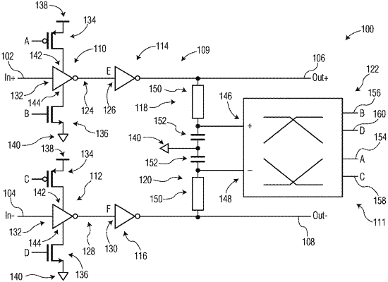
a differential signal inverter circuit including a first inverter circuit and a second inverter circuit, wherein the first inverter circuit includes a first differential signal input port and includes or is coupled at least indirectly to a first differential signal output port, and wherein the second inverter circuit includes a second differential signal input port and includes or is coupled at least indirectly to a second differential signal output port,
wherein each of the first inverter circuit and the second inverter circuit includes a respective inverter, a respective first transistor device coupled between the respective inverter and a first voltage, and a respective second transistor device coupled between the respective inverter and a second voltage, and wherein each of the first and second transistor devices includes a respective feedback input port; and
a feedback circuit coupled to the first and second differential signal output ports and also to the feedback input ports of the first and second transistor devices, wherein the feedback circuit includes an operational amplifier circuit including first and second amplifier input ports, a plurality of feedback output ports coupled at least indirectly with the respective feedback input ports, and at least one transconductance amplifier coupled between the amplifier input ports and the feedback output ports, and wherein the feedback circuit also includes first and second low pass filters respectively coupling the first and second differential signal output ports, respectively, with the first and second amplifier input ports, respectively, and
wherein the feedback circuit operates to provide one or more feedback signals from one or more of the feedback output ports to one or more of the feedback input ports based upon respective duty cycles exhibited by first and second output signals respectively provided at the first and second differential signal output ports, respectively, the one or more feedback signals causing one or more of the first and second transistor devices to perform current limiting depending upon a first difference between the respective duty cycles at a first time, wherein respective duty cycles of additional first and second output signals respectively provided at the first and second differential signal output ports at a second time subsequent to the first time are equal or substantially equal based on the current limiting, wherein the operational amplifier circuit additionally includes a plurality of additional circuit components that respectively couple the respective feedback output ports with one or both of the first and second voltages.
|