| CPC H03K 5/1252 (2013.01) [G01K 7/183 (2013.01); G01K 7/20 (2013.01); G01R 19/2506 (2013.01); G05F 1/648 (2013.01); G11C 7/02 (2013.01); G11C 7/1039 (2013.01); G11C 7/14 (2013.01); G11C 7/20 (2013.01); H03K 5/153 (2013.01); H03K 5/19 (2013.01); H03K 5/2472 (2013.01); H03K 17/223 (2013.01); H03K 17/24 (2013.01)] | 15 Claims |
|
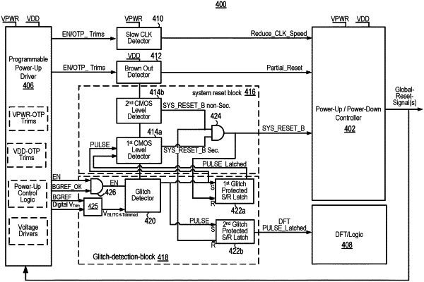
1. A circuit comprising:
a voltage-glitch-detection-block including:
a voltage-glitch-detector operable to detect a voltage-glitch in a supply voltage (VDD) and generate a voltage-glitch-detection-pulse (PULSE); and
a first latch having a set input coupled to the voltage-glitch-detector, the first latch operable to receive the PULSE and generate a first voltage-glitch-detection-pulse-latched (first PULSE_LATCHED) signal; and
a system reset block coupled the voltage-glitch-detector and the first latch to receive the PULSE and the first PULSE_LATCHED signal, and to generate a secure system reset signal that causes a number of on-chip-circuits in a chip including the circuit to be reset,
wherein the voltage-glitch-detector comprises:
a comparator having a first input coupled to VDD and a second input coupled to a reference voltage (VREF) based on a predetermined set-point voltage (VGLITCH), the comparator operable to compare VDD to VREF, and wherein the voltage-glitch-detector is operable to generate the PULSE when VDD<VREF; and
a first voltage-glitch-isolation filter (GIF) through which the comparator is coupled to VDD to provide a filtered voltage (VDDRC) to the comparator to isolate the comparator from a rapid decrease in VDD due to the voltage-glitch, and a second GIF through which the second input is coupled to VREF to isolate the comparator from a rapid change in VREF due to the voltage-glitch.
|