| CPC H03H 9/0552 (2013.01) [H03B 5/04 (2013.01); H03B 5/32 (2013.01); H03H 9/1021 (2013.01); H03H 9/19 (2013.01)] | 9 Claims |
|
1. A vibrator device comprising:
a base including a semiconductor substrate, which has a first surface and a second surface that is in a front-back relationship with the first surface, and an integrated circuit, which is disposed on the first surface or the second surface;
a vibrating element electrically coupled to the integrated circuit and disposed on a first surface side; and
a lid joined to the base at a joining portion of the base so as to accommodate the vibrating element,
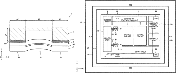
wherein the integrated circuit includes a reference voltage generation circuit that generates a reference voltage supplied to the integrated circuit,
the reference voltage generation circuit includes a resistance element,
the reference voltage generation circuit is disposed such that at least a part of the reference voltage generation circuit overlaps with the joining portion in a plan view from a direction orthogonal to the first surface, and
the resistance element is disposed in a region where the reference voltage generation circuit and the joining portion overlap in the plan view.
|