| CPC H03H 9/02913 (2013.01) [H03H 3/08 (2013.01); H03H 9/02559 (2013.01); H03H 9/02574 (2013.01); H03H 9/02834 (2013.01); H03H 9/131 (2013.01); H03H 9/54 (2013.01); H03H 9/6406 (2013.01); H03H 9/725 (2013.01); H10N 30/05 (2023.02); H10N 30/50 (2023.02); H10N 30/87 (2023.02)] | 20 Claims |
|
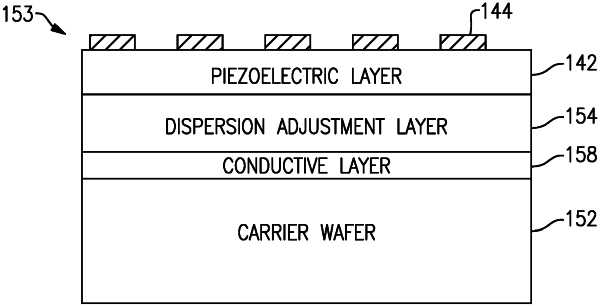
1. An acoustic wave device comprising:
a piezoelectric layer over a substrate;
an interdigital transducer electrode over the piezoelectric layer;
a conductive layer positioned between the piezoelectric layer and the substrate;
a grounding structure positioned under the substrate such that the substrate is positioned between the conductive layer and the grounding structure, the conductive layer being electrically connected to the grounding structure; and
an insulating layer disposed at least partially between the piezoelectric layer and the conductive layer.
|