| CPC H03F 3/2171 (2013.01) [H03F 3/185 (2013.01); H03F 2200/03 (2013.01)] | 19 Claims |
|
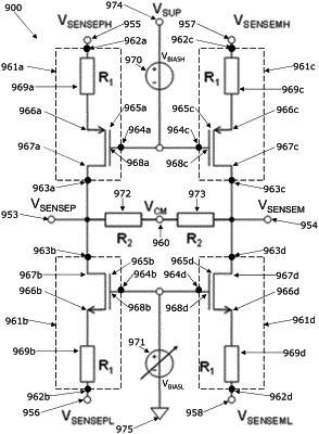
1. A sense amplifier circuit comprising:
a first-sensed-output-terminal;
a second-sensed-output-terminal;
a first-input-voltage-terminal;
a second-input-voltage-terminal;
a third-input-voltage-terminal;
a fourth-input-voltage-terminal;
a common-mode-voltage-node;
first-, second-, third- and fourth-amplification-blocks, each amplification-block comprising:
an amplification-block-input-node,
an amplification-block-output-node,
an amplification-block-control-node,
an amplification-block-transistor comprising:
a first-conduction-channel-terminal,
a second-conduction-channel-terminal that is connected to the amplification-block-output-node, and
a control-terminal that is connected to the amplification-block-control-node;
an amplification-block-resistor connected in series between the amplification-block-input-node and the first-conduction-channel-terminal,
a first-bias-voltage-source connected to the amplification-block-control-nodes of the first- and third-amplification-blocks;
a second-bias-voltage-source connected to the amplification-block-control-nodes of the second- and fourth-amplification-blocks;
a first-common-mode-voltage-resistor connected in series between the first-sensed-output-terminal and the common-mode-voltage-node; and
a second-common-mode-voltage-resistor connected in series between the second-sensed-output-terminal and the common-mode-voltage-node,
wherein:
the amplification-block-output-nodes of the first- and second-amplification-blocks are connected to the first-sensed-output-terminal;
the amplification-block-output-nodes of the third- and fourth-amplification-blocks are connected to the second-sensed-output-terminal;
the amplification-block-input-node of the first-amplification-block is connected to the first-input-voltage-terminal;
the amplification-block-input-node of the second-amplification-block is connected to the second-input-voltage-terminal;
the amplification-block-input-node of the third-amplification-block is connected to the third-input-voltage-terminal; and
the amplification-block-input-node of the fourth-amplification-block is connected to the fourth-input-voltage-terminal.
|