| CPC H02M 3/1584 (2013.01) [H02M 1/322 (2021.05); H02M 3/1552 (2021.05)] | 19 Claims |
|
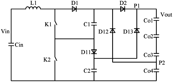
1. A three-level Boost circuit, comprising an input capacitor, an inductor, a first switch, a second switch, a first freewheeling diode, a second freewheeling diode, a flying capacitor, a balance capacitor, a charging diode, a clamp diode, a discharging diode and an output series capacitor bank, wherein
the output series capacitor bank comprises a plurality of output capacitors connected in series, and has a first node and a second node; a potential of the first node is higher than a potential of a cathode of the charging diode, and a potential difference between a cathode of the second freewheeling diode and the second node does not exceed a withstand voltage of the second freewheeling diode;
the input capacitor is connected in parallel with an input power supply; a negative electrode of the input capacitor is connected to a low potential end of the output series capacitor bank; a positive electrode of the input capacitor is coupled to a high potential end of the output series capacitor bank through a first terminal of the inductor, a second terminal of the inductor, an anode of the first freewheeling diode, a cathode of the first freewheeling diode, an anode of the second freewheeling diode and a cathode of the second freewheeling diode sequentially;
a second terminal of the inductor is coupled to the negative electrode of the input capacitor through a first terminal of the first switch, a second terminal of the first switch, a first terminal of the second switch and a second terminal of the second switch sequentially;
the cathode of the first freewheeling diode is coupled to the negative electrode of the input capacitor through a terminal of the flying capacitor, another terminal of the flying capacitor, an anode of the charging diode, a cathode of the charging diode, a terminal of the balance capacitor and another terminal of the balance capacitor sequentially;
the second terminal of the first switch is connected to the anode of the charging diode;
a cathode of the clamp diode is connected to the anode of the second freewheeling diode and an anode of the clamp diode is connected to the second node;
a cathode of the discharging diode is connected to the first node and an anode of the discharging diode is connected to the cathode of the charging diode;
a capacitance difference between the flying capacitor and the balance capacitor does not exceed a predetermined value; and
the first switch and the second switch are alternately switched on.
|