| CPC H02M 3/156 (2013.01) [H01L 23/49589 (2013.01); H01L 23/49811 (2013.01); H01L 23/49838 (2013.01); H01L 23/58 (2013.01)] | 20 Claims |
|
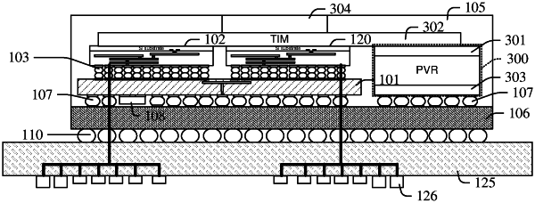
1. A semiconductor structure, comprising:
a first substrate including a first surface and a second surface opposite to the first surface;
a first die disposed over the second surface of the first substrate;
a second die disposed over the second surface of the first substrate and adjacent to the first die;
a plurality of first conductive bumps disposed between the first substrate and the first die and between the first substrate and the second die;
a second substrate disposed below the first surface of the first substrate;
a plurality of second conductive bumps disposed between the first substrate and the second substrate;
an in-package voltage regulator (PVR) chip disposed over the second substrate;
a molding material disposed over the first substrate and surrounding the first die, the second die, the plurality of first conductive bumps, the plurality of second conductive bumps, and the PVR chip; and
an integrated passive die (IPD) chip comprising a capacitive device disposed in one or more trenches in a semiconductor substrate of the IPD chip, the semiconductor substrate of the IPD chip being arranged between the first substrate and the second substrate and being laterally surrounded by the plurality of second conductive bumps.
|