| CPC H02M 1/4225 (2013.01) [H02M 1/0038 (2021.05); H02M 1/32 (2013.01)] | 14 Claims |
|
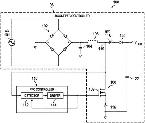
1. A process of operating a circuit having a transistor with a drain coupled to an inductor, the process comprising:
providing a drain voltage and a threshold voltage to first and second inputs of a comparator having a comparator output;
configuring the comparator to:
set the comparator output at a first level responsive to the drain voltage being greater than the threshold voltage; and
setting the comparator output at a second level responsive to the drain voltage being less than the threshold voltage;
providing the comparator output to an input of a blanking circuit, wherein the blanking circuit has a blanking circuit output;
coupling a timer circuit to the blanking circuit output, wherein the timer circuit includes a timer;
starting the timer for a timer period responsive to the first level changing to the second level;
sensing a current at the drain using a zero current detection circuit providing a zero current detection output signal in response to sensing a zero current through the drain;
setting an overvoltage signal responsive to the zero current detection output signal occurring during the timer period; and
setting a reduced on time of the transistor responsive to the zero current detection output signal occurring after the timer period expires.
|