| CPC H01S 5/2009 (2013.01) [H01S 5/04253 (2019.08); H01S 5/04254 (2019.08); H01S 5/11 (2021.01); H01S 5/185 (2021.01); H01S 5/2086 (2013.01); H01S 5/2095 (2013.01); H01S 5/320225 (2019.08); H01S 5/320275 (2019.08); H01S 5/34333 (2013.01); H01S 2301/176 (2013.01); H01S 2304/04 (2013.01)] | 7 Claims |
|
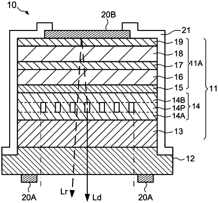
1. A manufacturing method for manufacturing a surface-emitting laser device made of a GaN-based semiconductor by an MOVPE method, the manufacturing method comprising steps of:
(a) growing a first cladding layer of a first conductive type on a substrate, with a {0001} plane as a growth plane;
(b) growing a guide layer of the first conductive type on the first cladding layer;
(c) forming holes in a surface of the guide layer by etching, the holes being two-dimensionally periodically arranged within a plane parallel to the guide layer;
(d) etching the guide layer by inductive coupled plasma reactive ion etching (ICP-RIE) using a chlorine-based gas and an argon gas;
(e) supplying a gas containing a nitrogen source to cause mass transport without supplying a group-III material gas, and then supplying the group-III material gas for growth, whereby a first embedding layer closing openings of the holes is formed to form a photonic crystal layer; and
(f) growing an active layer and a second cladding layer of a second conductive type in this order on the first embedding layer, the second conductive type being opposite to the first conductive type, wherein
the step (d) includes a step of referring to already-obtained data on a relationship of an attraction voltage and a ratio of the chlorine-based gas to the argon gas in the ICP-RIE with a diameter distribution of air holes embedded in the photonic crystal layer, and applying the attraction voltage and the ratio of the chlorine-based gas to the argon gas to the ICP-RIE on a basis of the data.
|