| CPC H01S 5/143 (2013.01) [G02B 6/12002 (2013.01); G02B 6/12004 (2013.01); G02B 6/34 (2013.01); G02B 6/4214 (2013.01); G02B 6/43 (2013.01); H01L 27/00 (2013.01); H01S 5/021 (2013.01); H01S 5/02251 (2021.01); H01S 5/1085 (2013.01); H01S 5/141 (2013.01); H01S 5/026 (2013.01); H01S 5/14 (2013.01); H01S 5/4025 (2013.01)] | 19 Claims |
|
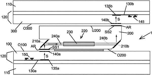
1. A photonic component (1) having at least one semiconductor laser amplifier (200) comprising at least one first mirror surface (210a) for coupling in and/or coupling out optical radiation (S), characterized in that
the first mirror surface (210a) of the semiconductor laser amplifier (200) is coupled to a photonic integrated chip (100),
wherein the chip (100) is arranged in such a way that it can emit optical radiation (S) from its chip top side (O100) in the direction of the first mirror surface (210a) and couple it into the semiconductor laser amplifier (200) and/or can receive at its chip top side (O100) radiation (S) amplified by the semiconductor laser amplifier (200) and coming from the first mirror surface (210a) and couple it into itself,
wherein the radiation (S) is emitted away from the chip top side (O100) in the direction of the first mirror surface (210a) at an angle of about 90°±20°, in particular perpendicular, to the chip top side (O100) and/or the radiation (S) coming from the first mirror surface (210a) is coupled into the chip (100) at an angle of about 90°±20°, in particular perpendicular, to the chip top side (O100);
wherein the chip (100) further comprises:
a substrate (110),
at least one integrated optical waveguide (130a) which is integrated in one or more waveguiding material layers of the chip (100) situated on the substrate (110),
a first coupler, in particular grating coupler (135a), which is formed in the optical waveguide (130a) or is connected to the optical waveguide (130a), and
at least one optical diffraction and refraction structure which is arranged in a region of the chip top side (O100) and which is integrated in one or more material layers of the chip (100) situated—as viewed from the substrate (110)—above the first coupler and carries out a beam shaping of the radiation (S) before coupling into the waveguide (130a) or after coupling out of the waveguide (130a) and wherein the at least one optical diffraction and refraction structure is a Fresnel lens having elliptic rings which are not circular and not arranged concentrically with respect to one another;
the component (1) comprises at least one first and one second photonic integrated chip (100, 300) which enclose the semiconductor laser amplifier (200) between them, in particular to form a sandwich structure,
the first mirror surface (210a) of the semiconductor laser amplifier (200) is coupled to the first chip (100) and a second mirror surface (210b) of the semiconductor laser amplifier (200) is coupled to a second chip (300); and
the first chip (100) comprises
wherein the at least one optical diffraction and refraction structure is radiation-connected to the first mirror surface (210a) of the semiconductor laser amplifier (200) and carries out a beam shaping of the radiation (S) after coupling out of the first waveguide (130a) and before emission at the chip top side (O100), and
the second chip (300) comprises
a second integrated optical waveguide (130b),
a second coupler which is formed in the second optical waveguide (130b) or is connected to the second optical waveguide (130b),
a second optical diffraction and refraction structure which is arranged in a region of the second chip top side (O300) and which is integrated in one or more material layers of the chip (300) situated—as viewed from the substrate (110) of the second chip (300)—above the second coupler and is radiation-connected to the second mirror surface (210b) of the semiconductor laser amplifier (200) and carries out a beam shaping of the radiation (S) amplified by the semiconductor laser amplifier (200) before coupling into the second coupler.
|