| CPC H01S 5/0428 (2013.01) [H01S 5/0421 (2013.01); H01S 5/06203 (2013.01); H01S 5/06216 (2013.01); H01S 2301/08 (2013.01)] | 6 Claims |

|
1. A narrow-pulse-width pulse laser, comprising:
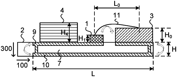
a circuit substrate, comprising:
a first conductor layer;
a second conductor layer; and
an insulating layer arranged between the first conductor layer and the second conductor layer, wherein the first conductor layer and the second conductor layer are electrically connected through a via hole in the insulating layer;
a laser chip;
one or more capacitors;
a field effect transistor;
wherein each of the field effect transistor, the one or more capacitors, and the laser chip is electrically connected to the circuit substrate;
wherein the one or more capacitors are arranged between the field effect transistor and the laser chip along an extension direction of a gap between the field effect transistor and the laser chip;
wherein the first conductor layer comprises a first conductor and the second conductor layer comprises a second conductor, where the first conductor and the second conductor are planar;
wherein each of the field effect transistor, the one or more capacitors, and the laser chip is electrically connected to the first conductor, wherein vertical projections of the field effect transistor, the one or more capacitors, and the laser chip on the circuit substrate are located in the first conductor; and
wherein along the extension direction of the gap between the field effect transistor and the laser chip, relationships among a width W1 of the laser chip, a total width W2 of the one or more capacitors, a width W0 of the field effect transistor and a width W of the first conductor satisfy that:
W1≤W0, W2≤W0, and W0≤W≤1.1W0,
wherein the one or more capacitors comprise a bare-die capacitor, and wherein the laser chip comprises a laser bare chip;
wherein the bare-die capacitor comprises a thin film silicon capacitor, and wherein the field effect transistor comprises a gallium nitride enhanced mode power transistor;
wherein the narrow-pulse-width pulse laser further comprises a gold wire;
wherein on one side far away from the circuit substrate, the bare-die capacitor and the laser bare chip are connected through the gold wire; and
an insulating paste that covers the bare-die capacitor, the laser bare chip, the gold wire, and bare areas of the field effect transistor and the circuit substrate to provide insulation protection.
|