| CPC H01Q 7/06 (2013.01) [H01Q 1/526 (2013.01); H04B 5/0037 (2013.01); H04B 5/0081 (2013.01); H04B 5/0087 (2013.01)] | 20 Claims |
|
1. A system comprising:
a substrate comprising a plurality of substrate layers including a first substrate layer within the plurality of substrate layers and other substrate layers;
an antenna structure, embedded within the plurality of substrate layers, the antenna structure comprising:
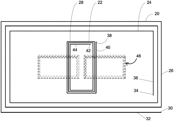
an outer coil comprising multiple layers of conductive wires, a plurality of turns, and two coil ends, wherein an innermost turn of the plurality of turns defines an inner perimeter of the outer coil; and
an inner coil array comprising at least three spaced-apart coils, wherein each of the at least three spaced-apart coils comprise multiple layers of conductive wires, a plurality of turns, and two coil ends, wherein the inner coil array resides within the inner perimeter of the outer coil,
wherein a first conductive layer of the multiple layers of the outer coil is disposed on a first side of the first substrate layer and a second conductive layer of the multiple layers of the outer coil is disposed on a second side of the first substrate layer,
wherein a first inner coil of the at least three spaced-apart coils comprises a first conductive layer and a second conductive layer, and the first conductive layer of the first inner coil is disposed on the first side of the first substrate layer and the second conductive layer of the first inner coil is disposed on the second side of the first substrate layer,
wherein the multiple layers of a second inner coil of the at least three spaced-apart coils are disposed on the other substrate layers positioned within the plurality of substrate layers below the first substrate layer, and
wherein the at least three spaced-apart coils are positioned in a stacked arrangement in which the first inner coil is at least partially overlaid on the second inner coil and a third inner coil of the at least three spaced-apart coils.
|