| CPC H01Q 3/36 (2013.01) | 19 Claims |
|
1. A scanning antenna, comprising:
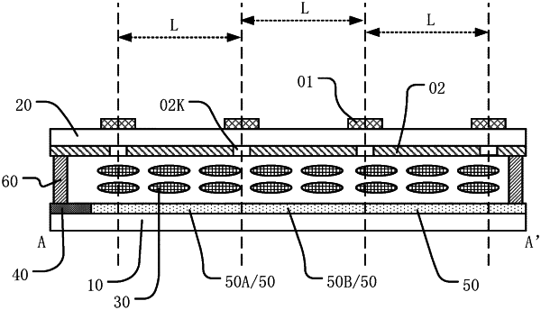
a first substrate and a second substrate, which are arranged oppositely;
a liquid crystal layer, between the first substrate and the second substrate;
a feed signal access terminal and a plurality of phase shift units, wherein the plurality of phase shift units is connected with each other, each phase shift unit is connected to the feed signal access terminal, and at least two phase shift units of the plurality of phase shift units have different electrical lengths with the feed signal access terminal; and
a load, wherein one end of the plurality of phase shift units which are connected with each other is connected to the feed signal access terminal, and the other end of the plurality of phase shift units which are connected with each other is connected to the load, and the load is one of a matched wave absorbing structure or a matched wave absorbing circuit component configured to absorb microwaves reaching the other end of the plurality of phase shift units.
|