| CPC H01L 33/12 (2013.01) [H01L 27/156 (2013.01); H01L 33/22 (2013.01); H01L 33/32 (2013.01); H01L 33/382 (2013.01); H01L 33/44 (2013.01)] | 4 Claims |
|
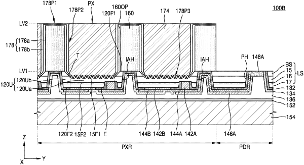
1. A semiconductor light-emitting device comprising:
a partition wall structure having an opening; and
a light-emitting structure comprising a buffer structure, an undoped semiconductor layer, a first-type semiconductor layer, an active layer, and a second-type semiconductor layer, which are stacked on the partition wall structure,
wherein the light-emitting structure further comprises a trench, which passes through the buffer structure and overlaps the opening of the partition wall structure,
wherein the buffer structure comprises a nucleation layer, a dislocation-removing structure, and a buffer layer, which are stacked on the partition wall structure,
wherein the dislocation-removing structure comprises a first material layer on the nucleation layer and a second material layer on the first material layer, the second material layer having a lattice constant different from a lattice constant of the first material layer, and
wherein a roughness of a surface of the first material layer in contact with the second material layer is higher than a roughness of a surface of the nucleation layer in contact with the first material layer and a roughness of a surface of the second material layer in contact with the buffer layer.
|