| CPC H01L 31/0725 (2013.01) [H01L 31/02008 (2013.01); H01L 31/03046 (2013.01); H01L 31/0504 (2013.01); H01L 31/0547 (2014.12); H01L 31/0687 (2013.01); H01L 31/078 (2013.01); H01L 31/0735 (2013.01); H01L 31/1844 (2013.01); Y02E 10/52 (2013.01); Y02E 10/544 (2013.01)] | 16 Claims |
|
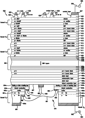
1. A multijunction solar cell comprising:
(a) a single monolithic semiconductor substrate having a top side and a bottom side opposite to the top side;
(b) a bottom solar subcell region in the semiconductor substrate including a nucleation layer deposited on the top side of the semiconductor substrate, the bottom solar subcell region having an emitter region and a base region disposed below the emitter region, the emitter region of the bottom solar subcell being on a portion of the semiconductor substrate and comprising atoms diffused from the nucleation layer into the semiconductor substrate from the top side thereof;
(c) an epitaxial semiconductor structure including a sequence of semiconductor epitaxial layers on the nucleation layer, the semiconductor structure including a first and second adjacent and parallel semiconductor regions with respect to incoming illumination, each of the first and second regions including an upper first solar subcell and a respective portion of the bottom solar subcell region; and
(d) an opening in the semiconductor substrate extending from the bottom side of the semiconductor substrate through the bottom solar subcell region and through a portion of the sequence of semiconductor layers and terminating at one or more of the semiconductor epitaxial layers grown on the nucleation layer, the multijunction solar cell being configured for illumination through a side of the multijunction solar cell that is opposite a side in which the opening is present,
the opening in the semiconductor substrate being a channel that divides the semiconductor substrate and a portion of the epitaxial semiconductor structure into the first and second parallel semiconductor regions, wherein the bottom solar subcell region is divided by the channel to form discrete, spaced-apart first and second bottom solar subcells (D1 and D2 respectively) in the respective first and second semiconductor regions, and
wherein the opening defines multiple ledges located, respectively, at different distances from the bottom side of the semiconductor substrate,
the multijunction solar cell further comprising at least one electrical contact pad on each of the ledges, and electrical interconnections connecting together respective ones of the electrical contact pads on different ones of the ledges.
|