| CPC H01L 29/7869 (2013.01) [H01L 21/02565 (2013.01); H01L 21/477 (2013.01); H01L 21/823412 (2013.01); H01L 21/823418 (2013.01); H01L 21/823462 (2013.01); H01L 27/1225 (2013.01); H01L 29/045 (2013.01); H01L 29/0847 (2013.01); H01L 29/24 (2013.01); H01L 29/4908 (2013.01); H01L 29/517 (2013.01); H01L 29/66742 (2013.01); H01L 29/66969 (2013.01); H01L 29/78621 (2013.01); H01L 29/78693 (2013.01); H01L 29/78696 (2013.01)] | 8 Claims |
|
1. A semiconductor device comprising:
a first transistor comprising:
a first terminal electrically connected to a first wiring;
a second terminal electrically connected to a second wiring; and
a third terminal;
a second transistor comprising:
a fourth terminal functioning as a gate of the second transistor electrically connected to the third terminal;
a fifth terminal electrically connected to a third wiring; and
a sixth terminal;
a third transistor comprising:
a seventh terminal electrically connected to the sixth terminal;
an eighth terminal electrically connected to a fourth wiring; and
a ninth terminal electrically connected to a fifth wiring;
wherein one of the first transistor, the second transistor, and the third transistor comprises:
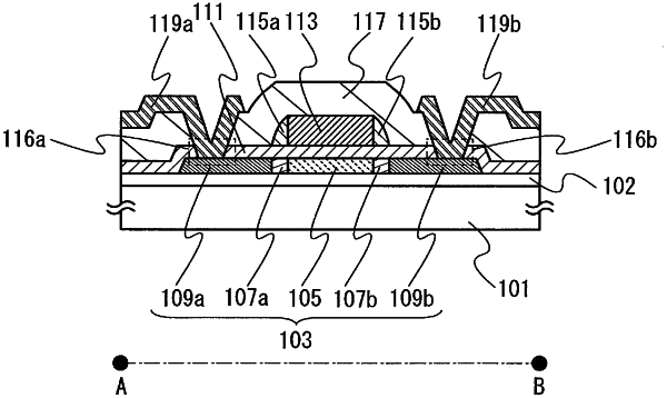
a first insulating layer;
an oxide semiconductor film over the first insulating layer comprising:
a first region;
a pair of second regions, the first region located between the pair of second regions; and
a pair of third regions, the first region and the pair of second regions located between the pair of third regions;
a gate insulating film over the oxide semiconductor film;
a gate electrode over the gate insulating film and overlapping with the first region;
a first electrode in contact with a top surface of the oxide semiconductor film; and
a second electrode in contact with the top surface of the oxide semiconductor film,
wherein the gate insulating film is in contact with a side surface of the oxide semiconductor film, a side surface of the first electrode, a side surface of the second electrode, and a top surface of the first insulating layer,
wherein the oxide semiconductor film comprises indium, gallium, and zinc,
wherein the gate insulating film extends beyond an end portion of the gate electrode and overlaps the first region and the pair of second regions,
wherein the gate insulating film is not in contact with a side surface of the gate electrode,
wherein the first region comprises a crystalline portion,
wherein the gate electrode, the first electrode, and the second electrode comprise copper, and
wherein a conductivity of the pair of third regions is higher than a conductivity of the pair of second regions.
|