| CPC H01L 29/7856 (2013.01) [H01L 21/845 (2013.01); H01L 27/1211 (2013.01); H01L 29/0653 (2013.01); H01L 29/42376 (2013.01); H01L 29/6653 (2013.01); H01L 29/6681 (2013.01); H01L 29/66553 (2013.01); H01L 29/36 (2013.01)] | 19 Claims |
|
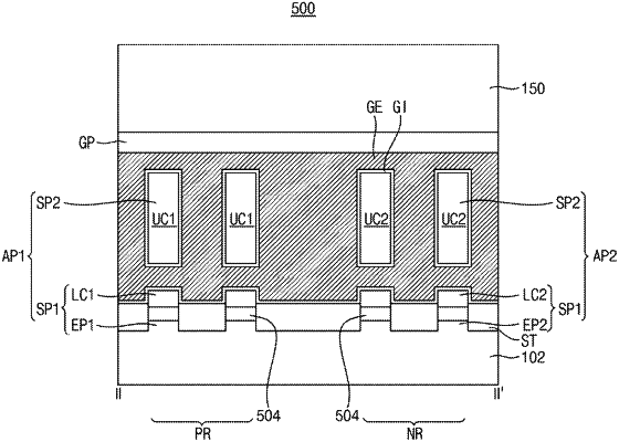
1. A semiconductor device, comprising:
a first semiconductor pattern on a substrate, the first semiconductor pattern including an extension pattern protruding from an upper surface of the substrate and a lower channel on the extension pattern;
a semiconductor oxide layer between the extension pattern and the lower channel;
a second semiconductor pattern on the first semiconductor pattern and spaced apart from the first semiconductor pattern in a vertical direction, the second semiconductor pattern including an upper channel extending in the vertical direction;
a gate electrode covering the lower channel and surrounding the upper channel; and
source/drain patterns on opposite sides of the upper channel,
wherein the substrate and the first semiconductor pattern are not intentionally doped such that the substrate and the first semiconductor pattern have a doping concentration of less than 1019/cm3.
|