| CPC H01L 29/7851 (2013.01) [H01L 29/0847 (2013.01); H01L 29/42392 (2013.01); H01L 29/78696 (2013.01)] | 20 Claims |
|
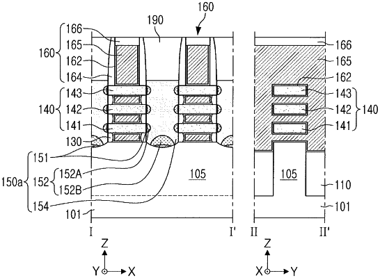
1. A semiconductor device, comprising:
an active region extending in a first direction on a substrate;
a plurality of channel layers on the active region and spaced apart from each other vertically;
a gate structure extending in a second direction on the substrate and surrounding the plurality of channel layers;
internal spacer layers covering side surfaces of the gate structure in the first direction in a lower portion of each of the plurality of channel layers, the internal spacer layers having internal side surfaces facing the gate structure and curved towards the gate structure in the first direction; and
a source/drain region on the active region at a side of the gate structure, the source/drain region being in contact with the plurality of channel layers and extending more upwardly than an uppermost surface of the plurality of channel layers, the source/drain region including:
first epitaxial layers including arsenic (As) and including first layers on side surfaces of the plurality of channel layers in the first direction and a second layer on the active region at a lower end of the source/drain region; and
a second epitaxial layer on the first epitaxial layer, the second epitaxial layer filling spaces between the first epitaxial layers and including phosphorus (P),
wherein the second layer has a first thickness in an edge region adjacent to the plurality of channel layers and has a second thickness, greater than the first thickness, in a center region in the first direction, and
wherein the gate structure includes a gate electrode having a first width in the first direction on the uppermost surface of the plurality of channel layers and having a second width in the first direction, greater than the first width, below the plurality of channel layers.
|