| CPC H01L 29/78391 (2014.09) [H01L 29/267 (2013.01); H01L 29/45 (2013.01); H01L 29/516 (2013.01); H01L 29/7606 (2013.01); H10K 10/466 (2023.02); H10K 10/472 (2023.02); H10K 10/84 (2023.02)] | 18 Claims |

|
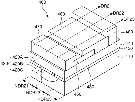
1. A negative differential resistance device, comprising:
a conductive substrate;
a dielectric layer comprising a first surface and a second surface opposing the first surface;
a first semiconductor layer comprising a first degenerated layer that is on the first surface of the dielectric layer and has a first polarity;
a second semiconductor layer comprising a second degenerated layer that comprises a region that overlaps the first semiconductor layer and has a second polarity;
a first electrode electrically connected to the first semiconductor layer;
a second electrode electrically connected to the second semiconductor layer;
a third electrode between the second surface of the dielectric layer and the conductive substrate, wherein the third electrode overlaps both the first semiconductor layer and the second semiconductor layer; and
an insulating layer between the second surface of the dielectric layer and the conductive substrate, in a region not overlapping the third electrode in a direction perpendicular to the second surface of the dielectric layer,
wherein the insulating layer does not overlap the third electrode in a region that overlaps both the first semiconductor layer and the second semiconductor layer.
|