| CPC H01L 29/7813 (2013.01) [H01L 29/0634 (2013.01); H01L 29/0878 (2013.01); H01L 29/407 (2013.01); H01L 29/66712 (2013.01); H01L 29/66734 (2013.01); H01L 29/7397 (2013.01); H01L 29/7802 (2013.01); H01L 29/1095 (2013.01)] | 5 Claims |
|
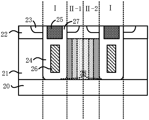
1. A semiconductor device structure, comprising:
a) a first semiconductor layer having dopants of a first type;
b) a second semiconductor layer having said dopants of said first type on said first semiconductor layer, wherein said second semiconductor layer is lightly-doped relative to said first semiconductor layer;
c) first column regions located in said second semiconductor layer;
d) a second column region located in said second semiconductor layer, wherein said second column region is at least arranged between two of said first column regions; and
e) a first sub-column region and a second sub-column region laterally arranged in said second column region, wherein a doping concentration of said first sub-column region decreases in a first lateral direction from a first of said two of said first column regions to said second sub-column region, and wherein a doping concentration of said second sub-column region decreases in a second lateral direction from a second of said two of said first column regions to said first sub-column region, wherein said first sub-column region and said second sub-column region have a same dopant type and together laterally extend a full distance between said two of said first column regions in order to increase a breakdown voltage and decrease an on-resistance, wherein said first sub-column region and said second sub-column region are heavily-doped relative to said second semiconductor layer, and wherein each of said first sub-column region and said second sub-column region extends from a top surface of said second semiconductor layer to a full depth of said first column regions.
|