| CPC H01L 29/7397 (2013.01) [H01L 29/0623 (2013.01); H01L 29/0649 (2013.01); H01L 29/0661 (2013.01); H01L 29/0696 (2013.01); H01L 29/083 (2013.01); H01L 29/401 (2013.01); H01L 29/407 (2013.01); H01L 29/4236 (2013.01); H01L 29/4238 (2013.01); H01L 29/42376 (2013.01); H01L 29/66348 (2013.01)] | 20 Claims |
|
1. A method comprising:
forming, in a substrate, a termination region of an insulated-gate bipolar transistor (IGBT) device, the termination region being included in an inactive region of the IGBT device, the inactive region at least partially surrounding an active region of the IGBT device;
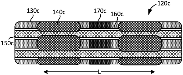
forming a trench in the substrate, the trench extending along a longitudinal axis in the active region of the IGBT device, the trench having:
a first sidewall included in a first mesa disposed in the active region of the IGBT device; and
a second sidewall included in a second mesa disposed in the active region of the IGBT device, the first mesa and the second mesa being parallel with the trench;
forming, in at least a portion of the first mesa in the active region of the IGBT device, an active segment of the IGBT device; and
forming, in at least a portion of the second mesa in the active region of the IGBT device, an inactive segment of the IGBT device, the inactive segment being defined by a dielectric material.
|