| CPC H01L 29/6656 (2013.01) [H01L 29/1033 (2013.01); H01L 29/42392 (2013.01); H01L 29/7851 (2013.01); H01L 29/7855 (2013.01); H01L 2029/7858 (2013.01)] | 20 Claims |
|
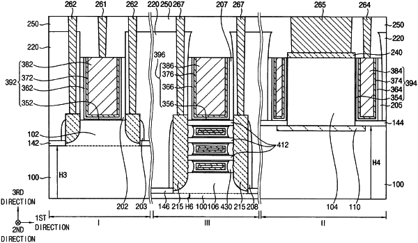
1. A semiconductor device, comprising:
a substrate including a first region and a second region,
a first transistor on the first region of the substrate, the first transistor including:
a first semiconductor pattern protruding from an upper surface of the first region of the substrate in a vertical direction;
a first gate structure covering an upper surface and a sidewall of the first semiconductor pattern; and
first source/drain layers on respective portions of the first semiconductor pattern at opposite sides of the first gate structure, upper surfaces of the first source/drain layers being closer to the substrate in the vertical direction than an uppermost surface of the first gate structure is to the substrate in the vertical direction; and
a second transistor on the second region of the substrate, the second transistor including:
a second semiconductor pattern protruding from an upper surface of the second region of the substrate in the vertical direction;
a second gate structure covering a sidewall of the second semiconductor pattern;
a second source/drain layer under the second semiconductor pattern at an upper portion of the second region of the substrate; and
a third source/drain layer on the second semiconductor pattern,
wherein the upper surface of the first region of the substrate is lower than the upper surface of the second region of the substrate.
|