| CPC H01L 29/66545 (2013.01) [H01L 23/544 (2013.01); H01L 27/10823 (2013.01); H01L 27/10876 (2013.01); H01L 27/10894 (2013.01); H01L 27/10897 (2013.01); H01L 27/1116 (2013.01); H01L 29/4236 (2013.01); H01L 27/11548 (2013.01); H01L 2223/5446 (2013.01)] | 20 Claims |
|
1. A semiconductor memory element comprising:
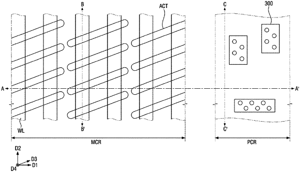
a substrate including a memory cell region and a peripheral circuit region;
an active region located in the memory cell region;
a gate pattern buried in the active region and including a gate electrode;
a conductive line disposed above the gate pattern;
a first region including a plurality of peripheral elements placed in the peripheral circuit region;
a dummy pattern buried in the peripheral circuit region;
a second region which includes the dummy pattern and does not overlap the first region; and
a conductive via disposed on the gate electrode, and connected to the gate electrode and the conductive line.
|