| CPC H01L 29/41741 (2013.01) [H01L 21/26513 (2013.01); H01L 21/765 (2013.01); H01L 29/407 (2013.01); H01L 29/66734 (2013.01); H01L 29/7813 (2013.01)] | 20 Claims |
|
1. A field-effect transistor (FET) comprising:
a semiconductor region;
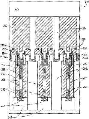
a trench disposed in the semiconductor region;
a trench gate disposed in an upper portion of the trench in an active region of the FET;
a conductive runner disposed in a bottom portion of the trench, the conductive runner being electrically coupled with a drain terminal of the FET via an ohmic contact with a heavily doped implant, a portion of the conductive runner being disposed in the active region below the trench gate; and
a dielectric layer disposed in the trench between trench gate and the conductive runner.
|