US 11,670,689 B2
Method for eliminating divot formation and semiconductor device manufactured using the same
Yu-Wen Tseng, Hsinchu (TW); Po-Wei Liu, Hsinchu (TW); Hung-Ling Shih, Hsinchu (TW); Tsung-Yu Yang, Hsinchu (TW); Tsung-Hua Yang, Hsinchu (TW); and Yu-Chun Chang, Hsinchu (TW)
Assigned to TAIWAN SEMICONDUCTOR MANUFACTURING COMPANY, LTD., Hsinchu (TW)
Filed by TAIWAN SEMICONDUCTOR MANUFACTURING COMPANY, LTD., Hsinchu (TW)
Filed on Sep. 10, 2021, as Appl. No. 17/471,722.
Claims priority of provisional application 63/184,936, filed on May 6, 2021.
Prior Publication US 2022/0359671 A1, Nov. 10, 2022
Int. Cl. H01L 29/40 (2006.01); H01L 29/423 (2006.01); H01L 29/06 (2006.01); H01L 29/78 (2006.01)
CPC H01L 29/401 (2013.01) [H01L 29/0653 (2013.01); H01L 29/423 (2013.01); H01L 29/7823 (2013.01)] 20 Claims
OG exemplary drawing
 
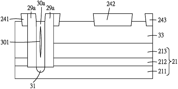
1. A method for eliminating divot formation, comprising:
forming an isolation layer;
forming a conduction layer which has an upper inclined boundary with the isolation layer such that the conduction layer has a portion located above a portion of the isolation layer at the upper inclined boundary;
etching back the isolation layer; and
etching back the conduction layer after etching back the isolation layer such that a top surface of the etched conduction layer is located at a level lower than a top surface of the etched isolation layer.