| CPC H01L 29/24 (2013.01) [C23C 16/4481 (2013.01); H01L 21/02565 (2013.01); H01L 21/02631 (2013.01); H01L 21/443 (2013.01); H01L 21/465 (2013.01); H01L 29/66969 (2013.01); H01L 29/7397 (2013.01); H01L 29/7806 (2013.01); H01L 29/7813 (2013.01); H02M 3/33576 (2013.01)] | 10 Claims |
|
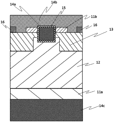
1. A semiconductor apparatus comprising:
a gate electrode;
an n type semiconductor layer including an oxide semiconductor as a major component, the oxide semiconductor containing a Group 13 metal of the periodic table; and
a channel layer formed of a channel directly or through other layers on a side wall of the gate electrode,
wherein a portion of or whole of the channel layer includes a p type oxide semiconductor,
wherein the p type oxide semiconductor includes a crystal of a metal oxide containing iridium or a mixed crystal of the metal oxide containing iridium.
|