| CPC H01L 29/1608 (2013.01) [H01L 29/1606 (2013.01); H01L 29/6603 (2013.01); H01L 29/66143 (2013.01); H01L 29/872 (2013.01)] | 20 Claims |
|
1. A device, comprising:
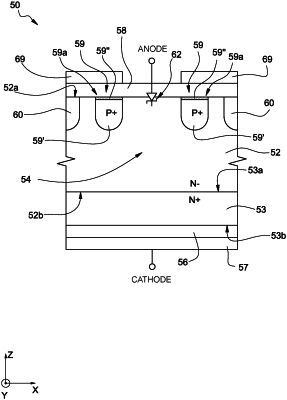
a merged PiN-Schottky (MPS) device that includes:
a solid body of SiC having a first conductivity type;
an implanted region at a first side of the solid body, which includes dopant species of a second conductivity type that is different from the first conductivity type, extends in depth in the solid body starting from the first side, and has a top surface co-planar with said first side of the solid body;
an ohmic contact region, which includes one or more carbon-rich layers having graphene, graphite, or a combination of graphene and graphite, and extends in the implanted region;
an anode metallization layer on the first side of the solid body, the anode metallization layer having a first face opposite the first side of the solid body; and
a passivation layer on the first face, the passivation layer including an opening that exposes a central region of the anode metallization layer, the passivation layer overlapping the ohmic contact region.
|