| CPC H01L 29/1087 (2013.01) [H01L 29/1095 (2013.01); H01L 29/66712 (2013.01); H01L 29/7802 (2013.01)] | 19 Claims |
|
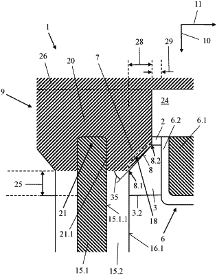
1. A semiconductor transistor device, comprising:
a source region;
a body region comprising a channel region extending in a vertical direction;
a drain region;
a gate region arranged aside the channel region in a lateral direction; and
a body contact region made of an electrically conductive material,
wherein the body contact region forms a body contact area,
wherein the body contact region is in electrical contact with the body region via the body contact area,
wherein the body contact area is tilted with respect to the vertical direction and the lateral direction,
wherein the body contact area has a concave shape in a vertical cross-section of the semiconductor transistor device.
|