| CPC H01L 29/1037 (2013.01) [H01L 29/0653 (2013.01); H01L 29/0665 (2013.01); H01L 29/0847 (2013.01); H01L 29/1608 (2013.01); H01L 29/42392 (2013.01); H01L 29/785 (2013.01); H01L 29/78696 (2013.01)] | 20 Claims |
|
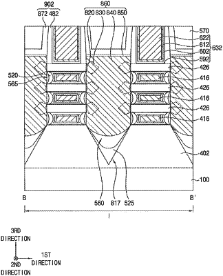
1. A semiconductor device, comprising;
an active pattern on a substrate, the active pattern including a recess on its upper surface;
gate structures on a first portion of the active pattern at a first side of the recess and a second portion of the active pattern at a second side of the recess;
channels spaced apart from each other in a vertical direction perpendicular to an upper surface of the substrate, each of the channels extending through one of the gate structures; and
a source/drain layer on the active pattern, the source/drain layer being connected to the channels and including a semiconductor material doped with impurities,
wherein an impurity concentration of the source/drain layer between the channels at the same level varies from a first sidewall of a first channel of the channels to a second sidewall of a second channel of the channels facing the first sidewall of the first channel, the impurity concentration having a first impurity concentration, a second impurity concentration, and the first impurity concentration in this order from the first sidewall to the second sidewall.
|