| CPC H01L 29/1033 (2013.01) [H01L 29/0615 (2013.01); H01L 29/7869 (2013.01); H01L 29/78642 (2013.01)] | 19 Claims |
|
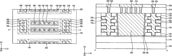
1. A semiconductor device comprising:
a gate electrode on a substrate:
a channel on the substrate, the channel surrounding sidewalls of the gate electrode; and
source/drain electrodes on the substrate at opposite sides of the gate electrode in a first direction parallel to an upper surface of the substrate,
wherein a thickness of the channel from the gate electrode to the source/drain electrodes in a horizontal direction is not constant but varies in a vertical direction, the horizontal direction being parallel to the upper surface of the substrate and the vertical direction being perpendicular to the upper surface of the substrate,
wherein the gate electrode is one of a plurality of gate electrodes spaced apart from each other in a second direction between the source/drain electrodes, and
wherein the second direction is parallel to the upper surface of the substrate and perpendicular to the first direction.
|