| CPC H01L 29/0665 (2013.01) [H01L 27/088 (2013.01); H01L 29/401 (2013.01); H01L 29/41733 (2013.01); H01L 29/42392 (2013.01); H01L 29/66545 (2013.01); H01L 29/66742 (2013.01); H01L 29/78696 (2013.01)] | 20 Claims |

|
1. A semiconductor device comprising:
a substrate;
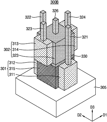
a 1st transistor formed above the substrate, and having a 1st transistor stack comprising a plurality of 1st channel structures, a 1st gate structure surrounding the 1st channel structures, and 1st and 2nd source/drain regions at both ends of the 1st transistor stack in a 1st channel length direction; and
a 2nd transistor formed above the 1st transistor in a vertical direction, and having a 2nd transistor stack comprising a plurality of 2nd channel structures, a 2nd gate structure surrounding the 2nd channel structures, and 3rd and 4th source/drain regions at both ends of the 2nd transistor stack in a 2nd channel length direction,
wherein the 3rd source/drain region vertically overlaps neither the 1st source/drain region nor the 2nd source/drain region, and the 4th source/drain region vertically overlaps neither the 1st source/drain region nor the 2nd source/drain region, and
wherein the 2nd channel structures of the 2nd transistor stack substantially overlap the 1st channel structures of the 1st transistor stack in a vertical direction.
|