| CPC H01L 29/0649 (2013.01) [H01L 21/823481 (2013.01); H01L 21/823878 (2013.01); H01L 27/088 (2013.01); H01L 27/092 (2013.01)] | 20 Claims |
|
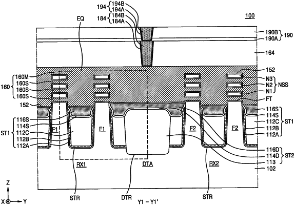
17. An integrated circuit device comprising:
a substrate comprising a first region and a second region spaced apart from each other, the substrate further comprising a first device isolation trench located in the first region and a second device isolation trench located in the second region;
a first fin-type active region defined by the first device isolation trench in the first region;
at least one nanosheet on a first fin top surface of the first fin-type active region and spaced apart from the first fin top surface in a vertical direction;
a second fin-type active region defined by the second device isolation trench in the second region and comprising a second fin top surface higher, relative to a bottom surface of the substrate, than the first fin top surface;
a first insulating structure on a sidewall of the first fin-type active region in the first region; and
a second insulating structure on a sidewall of the second fin-type active region in the second region,
wherein each of the first insulating structure and the second insulating structure comprises:
a first insulating liner in contact with the substrate;
a second insulating liner on the first insulating liner and comprising an uppermost portion at a second level that is lower, relative to the bottom surface of the substrate, than a first level of the first fin top surface;
a lower buried insulating layer on the second insulating liner and comprising a first top surface at a third level that is lower, relative to the bottom surface of the substrate, than the second level; and
an upper buried insulating layer on the uppermost portion of the second insulating liner and the first top surface of the lower buried insulating layer and comprising a second top surface at a fourth level that is equal to or higher, relative to the bottom surface of the substrate, than the second level.
|