| CPC H01L 28/75 (2013.01) [H01L 27/101 (2013.01); H01L 27/10805 (2013.01); H01L 27/10808 (2013.01); H01L 27/10811 (2013.01); H01L 27/10814 (2013.01); H01L 27/10847 (2013.01); H01L 27/10852 (2013.01); H01L 27/10855 (2013.01)] | 19 Claims |
|
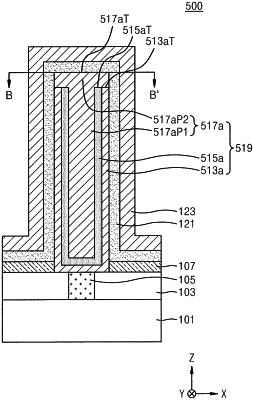
1. A semiconductor device comprising:
a substrate;
a lower electrode structure disposed on the substrate;
a dielectric layer disposed on the lower electrode structure; and
an upper electrode structure disposed on the dielectric layer,
wherein:
the lower electrode structure comprises:
a first lower electrode pattern having a first recess;
a second lower electrode pattern disposed in the first recess of the first lower electrode pattern and having a second recess; and
a third lower electrode pattern fully filling the second recess of the second lower electrode pattern,
the first lower electrode pattern is cylinder-shaped,
the second lower electrode pattern is cylinder-shaped, and
the dielectric layer contacts the first lower electrode pattern, the second lower electrode pattern and the third lower electrode pattern.
|