| CPC H01L 27/156 (2013.01) [H01L 33/0093 (2020.05); H01L 33/0095 (2013.01); H01L 33/007 (2013.01)] | 20 Claims |
|
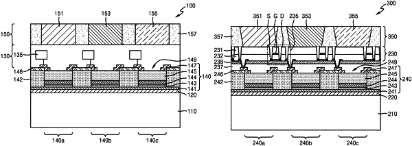
1. A micro light emitting diode (LED) device, comprising:
a support substrate;
a light emitting layer provided on the support substrate, the light emitting layer comprising:
a stacked structure including a first semiconductor layer, an active layer, and a second semiconductor layer;
a first electrode and a second electrode provided on a first side and a second side of the stacked structure, respectively; and
a plurality of light emitting regions;
a bonding layer between the support substrate and the light emitting layer; and
a drive layer provided on the light emitting layer and comprising a drive element, the drive element being electrically connected to the light emitting layer and configured to apply power to the plurality of light emitting regions of the light emitting layer,
wherein the support substrate is a separate substrate from a growth substrate on which the stacked structure of the light emitting layer is formed through a semiconductor deposition process, and the bonding layer is formed between the support substrate and the light emitting layer by bonding the support substrate to the growth substrate.
|