| CPC H01L 27/14679 (2013.01) [H01L 27/1461 (2013.01); H01L 27/1462 (2013.01); H01L 27/14612 (2013.01); H01L 27/14683 (2013.01); H01L 31/035218 (2013.01); H01L 31/1129 (2013.01)] | 6 Claims |
|
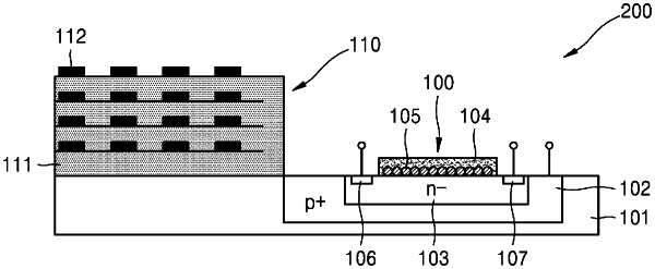
1. An opto-electronic device comprising:
a semiconductor substrate;
a light receiving unit formed in the semiconductor substrate; and
a driving circuit arranged on a surface of the semiconductor substrate at a portion of the semiconductor substrate not overlapping the light receiving unit in a plan view, wherein
the light receiving unit comprises:
a first semiconductor layer arranged in an upper region of the semiconductor substrate and doped with a first conductivity type impurity;
a second semiconductor layer arranged on the first semiconductor layer and doped with a second conductivity type impurity different from the first conductivity type impurity;
a transparent matrix layer arranged on an upper surface of the second semiconductor layer;
a plurality of quantum dots arranged to contact the transparent matrix layer; and
a first electrode arranged on a first side of the transparent matrix layer and a second electrode arranged on a second side of the transparent matrix layer opposite to the first side, wherein the first electrode and the second electrode are electrically connected to the second semiconductor layer,
wherein the first semiconductor layer is doped to have a first doping concentration and the second semiconductor layer is doped to have a second doping concentration less than the first doping concentration.
|