| CPC H01L 27/1463 (2013.01) [H01L 27/1462 (2013.01); H01L 27/14645 (2013.01); H01L 27/14685 (2013.01)] | 14 Claims |
|
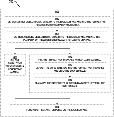
1. A method for forming an image sensor with passivated full deep-trench isolation, comprising:
forming a plurality of trenches in a front surface of a semiconductor substrate, each of the plurality of trenches having a trench depth;
filling the plurality of trenches with a sacrificial material;
forming a plurality of photodiode regions in the semiconductor substrate, each pair of adjacent photodiode regions being separated by a trench of the plurality of trenches;
forming a circuit layer disposed on the front surface of the semiconductor substrate; and
thinning the semiconductor substrate by removing material from a back surface of the semiconductor substrate until the semiconductor substrate has a thickness less than the trench depth, the back surface being opposite the front surface; and
removing the sacrificial material.
|