| CPC H01L 27/1463 (2013.01) [H01L 27/14603 (2013.01); H01L 27/14621 (2013.01); H01L 27/14627 (2013.01); H01L 27/14636 (2013.01); H01L 27/14689 (2013.01)] | 20 Claims |
|
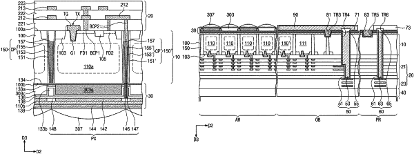
1. An image sensor, comprising:
a substrate having a first surface and an opposing second surface and including unit pixels respectively having photoelectric conversion regions;
a semiconductor pattern disposed in a first trench defining the unit pixels, the semiconductor pattern including a first semiconductor layer provided on an inner surface of the first trench and a second semiconductor layer provided on the first semiconductor layer; and
a first contact provided on the second surface and connected to the semiconductor pattern,
wherein a height of the first semiconductor layer from a bottom surface of the first trench is less than a height of the second semiconductor layer from the bottom surface of the first trench.
|