| CPC H01L 27/1463 (2013.01) [H01L 27/14605 (2013.01); H01L 27/14612 (2013.01); H01L 27/14623 (2013.01); H01L 27/14627 (2013.01); H01L 27/14645 (2013.01); H01L 27/14689 (2013.01); H01L 27/14812 (2013.01)] | 18 Claims |
|
1. A pixel array included in an auto-focus image sensor,
comprising:
a substrate including a first surface and a second surface opposite to the first surface, a gate electrode being disposed on the first surface;
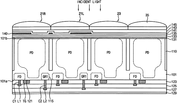
a plurality of pixels in the substrate, the plurality of pixels including a plurality of first pixels configured to detect a phase difference and a plurality of second pixels configured to detect an image;
a deep device isolation region in the substrate, the deep device isolation region extending substantially vertically from a first end of the deep device isolation region to a second end of the deep device isolation region to isolate the plurality of pixels from each other, the first end being in contact with the second surface and the second end not being in contact with the first surface;
a plurality of first ground regions adjacent to the first surface in the substrate, each of the plurality of first ground regions being included in a corresponding one of the plurality of first pixels; and
a light shielding pattern on the second surface of the substrate, the light shielding pattern being configured such that an amount of first light incident on each of the plurality of first pixels being smaller than an amount of second light incident on each of the plurality of second pixels,
wherein a ground voltage is applied to each of the plurality of first ground regions through a contact from a signal line formed on the first surface of the substrate, and the ground voltage applied to each of the plurality of first ground regions is transferred to at least some of the plurality of second pixels via a space between the deep device isolation region and the first surface of the substrate,
wherein the space is provided between the second end of the deep device isolation region and the first surface, and
wherein the at least some of the plurality of second pixels do not include any ground region.
|