| CPC H01L 27/14623 (2013.01) [H01L 27/14621 (2013.01); H04N 25/77 (2023.01)] | 7 Claims |
|
1. An imaging element comprising:
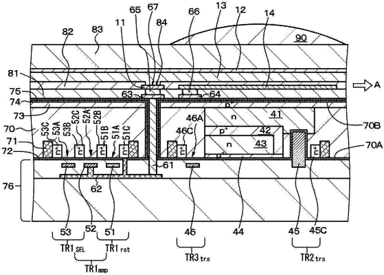
a photoelectric conversion unit including a first electrode, a photoelectric conversion layer, and a second electrode that are stacked; and
a semiconductor substrate, wherein
the photoelectric conversion unit is arranged on an upper side of the semiconductor substrate, the photoelectric conversion unit further includes a charge storage electrode arranged apart from the first electrode, arranged to face the photoelectric conversion layer through an insulating layer, and arranged between the second electrode and the semiconductor substrate in a depth direction of the semiconductor substrate, and wherein a top of the charge storage electrode is arranged at same level as a top of the first electrode in the depth direction of the semiconductor substrate,
when photoelectric conversion occurs in the photoelectric conversion layer after light enters the photoelectric conversion layer, an absolute value of a potential applied to a part of the photoelectric conversion layer facing the charge storage electrode is a value larger than an absolute value of a potential applied to a region of the photoelectric conversion layer positioned between the imaging element and an adjacent imaging element.
|