| CPC H01L 27/1462 (2013.01) [G02B 1/111 (2013.01); G02B 5/20 (2013.01); H01L 27/14605 (2013.01); H01L 27/14627 (2013.01)] | 19 Claims |
|
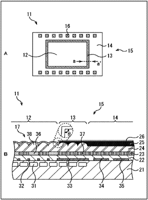
1. An imaging element, comprising:
a first light absorbing film formed in an effective pixel peripheral region, the effective pixel peripheral region being provided so as to enclose an outer side of an effective pixel region in which a plurality of pixels is disposed in a matrix formed in a semiconductor substrate;
a microlens layer, wherein the microlens layer is on a light incident surface side of the first light absorbing film, wherein the microlens layer includes a plurality of microlenses, and wherein the microlenses are formed so as to condense light for each of the pixels in the effective pixel region; and
a second light absorbing film formed in the effective pixel peripheral region, wherein the second light absorbing film is on a light incident surface side of the microlens layer, wherein, in a plan view, at least a portion of the first light absorbing film, at least a portion of the microlens layer, and at least a portion of the second light absorbing film overlap each other in the effective pixel peripheral region, and wherein an edge portion of the second light absorbing film has an angular portion when viewed in cross section.
|