| CPC H01L 27/14612 (2013.01) [H01L 27/14636 (2013.01); H01L 27/14643 (2013.01); H01L 27/14831 (2013.01); H01L 27/14679 (2013.01)] | 20 Claims |
|
1. An image sensing device comprising:
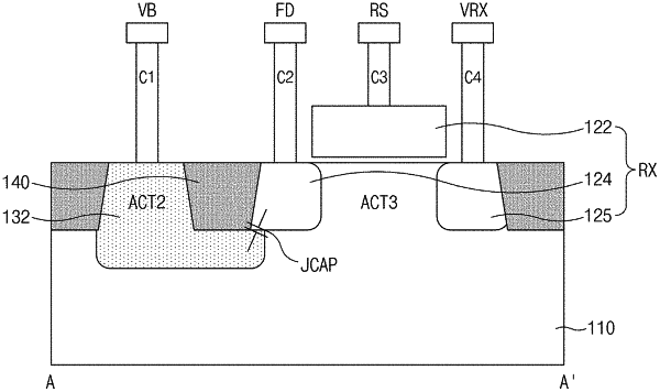
a substrate structured to include a first surface on a first side of the substrate and a second surface on a second side of the substrate opposite to the first side and to further include a first active region and a second active region in a portion of the substrate near the second surface;
at least one photoelectric conversion element formed in the substrate, and structured to generate photocharges by performing photoelectric conversion of incident light received through the first surface of the substrate;
a floating diffusion region formed near the second surface of the substrate and structured to receive the photocharges from the photoelectric conversion element and temporarily store the received photocharges;
a transistor formed in the first active region, and structured to include a first source/drain region coupled to the floating diffusion region; and
a well pickup region formed in the second active region, and structured to apply a bias voltage to the substrate,
wherein the first source/drain region and the well pickup region have complementary conductivities and are formed to be in contact with each other.
|