US 11,670,652 B2
Imaging device including a photoelectric converter and a capacitive element having a dielectric film sandwiched between electrodes and a mode switching transistor
Masashi Murakami, Kyoto (JP); Kazuko Nishimura, Kyoto (JP); Yutaka Abe, Osaka (JP); Yoshiyuki Matsunaga, Kyoto (JP); Yoshihiro Sato, Osaka (JP); and Junji Hirase, Osaka (JP)
Assigned to PANASONIC INTELLECTUAL PROPERTY MANAGEMENT CO., LTD., Osaka (JP)
Filed by Panasonic Intellectual Property Management Co., Ltd., Osaka (JP)
Filed on Apr. 4, 2022, as Appl. No. 17/712,873.
Application 17/712,873 is a continuation of application No. 16/945,636, filed on Jul. 31, 2020, granted, now 11,329,079.
Application 16/945,636 is a continuation of application No. 16/401,974, filed on May 2, 2019, granted, now 10,770,491, issued on Sep. 8, 2020.
Application 16/401,974 is a continuation of application No. 15/878,902, filed on Jan. 24, 2018, granted, now 10,325,945, issued on Jun. 18, 2019.
Application 15/878,902 is a continuation of application No. 14/972,153, filed on Dec. 17, 2015, granted, now 9,917,119, issued on Mar. 13, 2018.
Claims priority of application No. 2014-264694 (JP), filed on Dec. 26, 2014; application No. 2014-264695 (JP), filed on Dec. 26, 2014; application No. 2015-167556 (JP), filed on Aug. 27, 2015; and application No. 2015-207381 (JP), filed on Oct. 21, 2015.
Prior Publication US 2022/0320161 A1, Oct. 6, 2022
Int. Cl. H01L 27/146 (2006.01); H01L 51/42 (2006.01)
CPC H01L 27/14609 (2013.01) [H01L 27/14632 (2013.01); H01L 27/14643 (2013.01); H01L 27/14665 (2013.01); H01L 27/14636 (2013.01); H01L 51/42 (2013.01)] 18 Claims
OG exemplary drawing
 
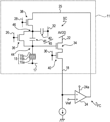
1. An imaging device comprising:
a photoelectric converter that converts incident light into a signal charge;
a node to which the signal charge is input;
a transistor having a source and a drain, one of the source and the drain being connected to the node; and
a capacitive element including a first electrode, a second electrode and a dielectric film sandwiched between the first electrode and the second electrode, the first electrode being connected to the other of the source and the drain of the transistor, the second electrode being connected to a voltage source or a ground, wherein
the transistor is configured to switch a first mode and a second mode, a sensitivity in the first mode being different from a sensitivity in the second mode.