| CPC H01L 27/14605 (2013.01) [G01S 7/4863 (2013.01); G01S 17/894 (2020.01); H01L 27/1463 (2013.01); H01L 27/14629 (2013.01); H01L 27/14634 (2013.01); H01L 27/14636 (2013.01); H01L 27/14665 (2013.01); H04N 25/702 (2023.01); H04N 25/79 (2023.01)] | 6 Claims |
|
1. A sensor chip, comprising:
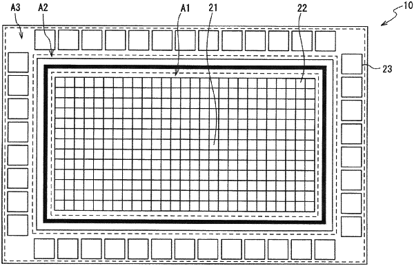
a pixel array section including a pixel area in which a plurality of pixels is arranged in rows and columns;
an avalanche photodiode element that amplifies a carrier by a high electric field area provided for the each of the pixels;
an inter-pixel separation section that insulates and separates the each of the pixels from another pixel adjacent to the each of the pixels in a semiconductor substrate in which the avalanche photodiode element is formed; and
a wiring that is arranged in a wiring layer laminated on a surface being opposite to a light receiving surface of the semiconductor substrate in such a way as to cover at least the high electric field area,
wherein the pixel array section includes a dummy pixel area located near a peripheral edge of the pixel area, and
a cathode electric potential and an anode electric potential of the avalanche photodiode element that is arranged in the dummy pixel area are a same electric potential, or at least one of the cathode electric potential and the anode electric potential is in a floating state.
|