| CPC H01L 27/1244 (2013.01) [H01L 27/1237 (2013.01); H01L 27/1259 (2013.01)] | 11 Claims |
|
1. A display substrate, comprising:
a substrate, comprising a plurality of pixel island regions spaced apart and a plurality of bridge regions connecting adjacent pixel island regions;
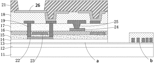
thin film transistors, disposed in the pixel island regions, wherein the thin film transistors comprise an active layer, a first gate insulating layer, a first gate, a second gate insulating layer, a second gate, a dielectric layer, and a source/drain layer which are disposed on the substrate and sequentially laminated;
first signal lines, disposed in the pixel island regions; and
first connecting bridges, disposed in the bridge regions;
wherein the first signal lines are electrically connected to the first or second gates of the thin film transistors, the first connecting bridges are connected to the first signal lines in the adjacent pixel island regions along a first direction, and the first connecting bridges and the first signal lines are disposed in a same layer as the gates of the thin film transistors;
the first signal lines extends along the first direction, the first connecting bridges, the first signal lines, and the gate are all made of an aluminum alloy and have an elongation at break of 1.5% to 3%, and the first and second gates have a thickness of 300 nm to 500 nm along a direction perpendicular to the bearing surface of the substrate; and
the display substrate further comprises second connecting bridges disposed in the bridge regions and second signal lines disposed in the pixel island regions, wherein the second signal lines are electrically connected to the sources/drains of the thin film transistors and extend along the second direction; the second connecting bridges are electrically connected to the second signal lines in the adjacent pixel island regions along the second direction; both the second connecting bridges and the second signal lines are disposed in the same layer as the sources/drains of the thin film transistors; and the first direction is perpendicular to the second direction.
|
|
10. A display device, comprising a display substrate and a driving module, wherein
the display substrate comprises a substrate, thin film transistors, first signal lines, and first connecting bridges; wherein the substrate comprises a plurality of pixel island regions spaced apart and a plurality of bridge regions connecting adjacent pixel island regions, the thin film transistors are disposed in the pixel island regions, and the thin film transistors comprise an active layer, a first gate insulating layer, a first gate, a second gate insulating layer, a second gate, a dielectric layer, and a source/drain layer which are disposed on the substrate and sequentially laminated, the first signal lines are disposed in the pixel island regions, the first connecting bridges are disposed in the bridge regions, the first signal lines are electrically connected to first or second gates of the thin film transistors, the first connecting bridges are connected to the first signal lines in the adjacent pixel island regions along a first direction, and the first connecting bridges and the first signal lines are disposed in the same layer as the first and second gates of the thin film transistors; the first signal lines extends along the first direction, the first connecting bridges, the first signal lines, and the first and second gates are all made of an aluminum alloy and have an elongation at break of 1.5% to 3%, and the first and second gates has a thickness of 300 nm to 500 nm along a direction perpendicular to the bearing surface of the substrate; and the display substrate further comprises second connecting bridges disposed in the bridge regions and second signal lines disposed in the pixel island regions, wherein the second signal lines are electrically connected to the sources/drains of the thin film transistors and extend along the second direction; the second connecting bridges are electrically connected to the second signal lines in the adjacent pixel island regions along the second direction; both the second connecting bridges and the second signal lines are disposed in the same layer as the sources/drains of the thin film transistors; and the first direction is perpendicular to the second direction; and
the driving module is electrically connected to the first signal lines and configured to provide a driving signal for the first signal lines.
|