| CPC H01L 27/124 (2013.01) [G09G 3/32 (2013.01); G09G 2300/0426 (2013.01); G09G 2300/0809 (2013.01); G09G 2310/0243 (2013.01); G09G 2310/0267 (2013.01); H01L 27/156 (2013.01); H01L 27/3211 (2013.01); H01L 27/3262 (2013.01); H01L 27/3265 (2013.01); H01L 27/3276 (2013.01)] | 12 Claims |
|
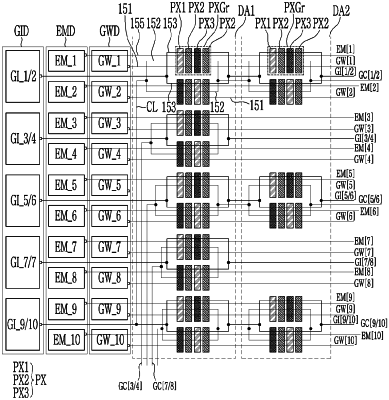
1. A display device, comprising
a first region and a second region each including a plurality of pixels, and
an optical sensor disposed in the second region,
wherein each of the plurality of pixels includes:
a light emitting diode (LED) connected between a driving voltage line and a common voltage line;
a driving transistor connected between the driving voltage line and the light emitting diode (LED);
a second transistor connected between a first electrode of the driving transistor and a data line, the first electrode of the driving transistor being connected to the driving voltage line; and
a storage capacitor connected between the driving voltage line and a gate electrode of the driving transistor, and
wherein a ratio of a width to a length of a channel of the driving transistor for the second region is 155% or more and 206% or less of a ratio of a width to a length of a channel of the driving transistor for the first region.
|