| CPC H01L 27/124 (2013.01) [H01L 27/1259 (2013.01); B60K 35/00 (2013.01); B60K 2370/785 (2019.05)] | 7 Claims |
|
1. A transparent display, wherein the transparent display is an organic light emitting diode (OLED) display and comprises:
a substrate and a plurality of frame traces;
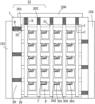
wherein the substrate comprises a transparent display region and a frame region defined on a left side, a right side, and an upper side of the transparent display region, and the transparent display region and the frame region are transparent;
wherein the plurality of frame traces are disposed in the frame region, and each frame trace comprises a hollow portion and a conductive portion surrounding the hollow portion, and a ratio of an area of the hollow portion to an area of the conductive portion is greater than 1.5 in each frame trace;
wherein the plurality of frame traces comprise a plurality of first frame traces disposed in a first metal layer and a plurality of second frame traces disposed in a second metal layer, and an insulating layer is provided between the first metal layer and the second metal layer;
wherein the transparent display region is provided with a plurality of data lines arranged at intervals and a plurality of scan lines arranged at intervals and intersecting the plurality of data lines, the plurality of data lines are disposed in the second metal layer, and the plurality of scan lines are disposed in the first metal layer;
wherein each scan line in odd rows of the plurality of scan lines is electrically connected to a respective one of the plurality of first frame traces on the left side of the transparent display region, each scan line in even rows of the plurality of scan lines is electrically connected to a respective one of the plurality of first frame traces on the right side of the transparent display region, and each data line is electrically connected to a respective one of the plurality of second frame traces on the upper side of the transparent display region; and
wherein the first frame traces on the left side of the transparent display region are electrically connected to a first gate driver, and the first frame traces on the right side of the transparent display region are electrically connected to a second gate driver, and the plurality of second frame traces are electrically connected to a source driver.
|