| CPC H01L 27/0924 (2013.01) [H01L 29/7851 (2013.01)] | 20 Claims |
|
1. A semiconductor device comprising:
a substrate;
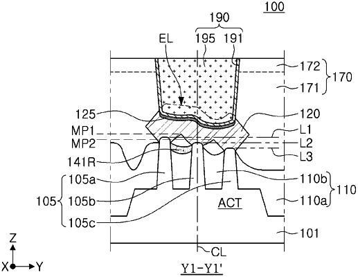
a plurality of active fins on an active region of the substrate, the plurality of active fins extending in a first direction, spaced apart from each other in a second direction intersecting the first direction, and having upper surfaces of different respective heights;
a gate structure extending in the second direction and traversing the plurality of active fins;
a device isolation film on an upper surface of the active region and side surfaces of the plurality of active fins;
a source/drain region on the plurality of active fins, on at least one side of the gate structure, and including an epitaxial layer on the plurality of active fins;
an insulating spacer on an upper surface of the device isolation film and having a lateral asymmetry with respect to a center line of the source/drain region in a cross section taken along the second direction;
an interlayer insulating region on the device isolation film and on the gate structure and the source/drain region; and
a contact structure in the interlayer insulating region and electrically connected to the source/drain region,
wherein the plurality of active fins include a first active fin and a second active fin,
wherein the first active fin has an upper surface higher than an upper surface of the second active fin, and
wherein the insulating spacer is on a first portion of the upper surface of the device isolation film, adjacent to the first active fin, and is not on a second portion of the upper surface of the device isolation film, adjacent to an outer side of the second active fin.
|