| CPC H01L 25/18 (2013.01) [H01L 23/3128 (2013.01); H01L 23/481 (2013.01); H01L 23/49811 (2013.01); H01L 23/49822 (2013.01); H01L 23/5226 (2013.01); H01L 23/66 (2013.01); H01L 24/20 (2013.01); H01L 24/16 (2013.01); H01L 2223/6677 (2013.01); H01L 2224/16227 (2013.01)] | 20 Claims |
|
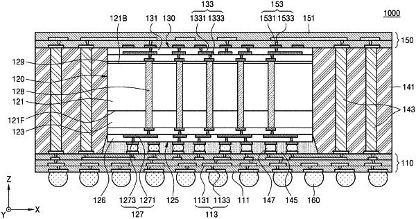
1. A semiconductor package comprising:
a first redistribution structure comprising a first redistribution pattern;
a first semiconductor chip on the first redistribution structure, the first semiconductor chip comprising a semiconductor substrate, a first back end of line (BEOL) structure on a first surface of the semiconductor substrate and comprising a first interconnect pattern insulated by a plurality of first interlayer insulating layers, and a second BEOL structure on a second surface of the semiconductor substrate and comprising a second interconnect pattern insulated by a plurality of second interlayer insulating layers;
a molding layer on the first redistribution structure and covering a sidewall of the first semiconductor chip;
a second redistribution structure on the first semiconductor chip and the molding layer, the second redistribution structure comprising a second redistribution pattern electrically connected to the second interconnect pattern of the second BEOL structure; and
a conductive post passing through the molding layer and electrically connecting the first redistribution pattern to the second redistribution pattern,
wherein a footprint of the second BEOL structure is the same as a footprint of the first semiconductor chip and smaller than a footprint of the second redistribution structure, and
the first semiconductor chip is configured to receive at least one of a power/ground signal or an input data signal through a first electrical path and a remainder of the power/ground signal or the input data signal through a second electrical path,
the first electrical path including the first redistribution structure, the first BEOL structure, and the second electrical path including the first redistribution structure, the conductive post, the second redistribution structure, and the second BEOL structure.
|