| CPC H01L 25/167 (2013.01) [H01L 24/08 (2013.01); H01L 24/32 (2013.01); H01L 27/1469 (2013.01); H01L 27/14634 (2013.01); H01L 27/14636 (2013.01); H01L 2224/08145 (2013.01); H01L 2224/08221 (2013.01); H01L 2224/32145 (2013.01)] | 8 Claims |
|
1. An imaging unit, comprising
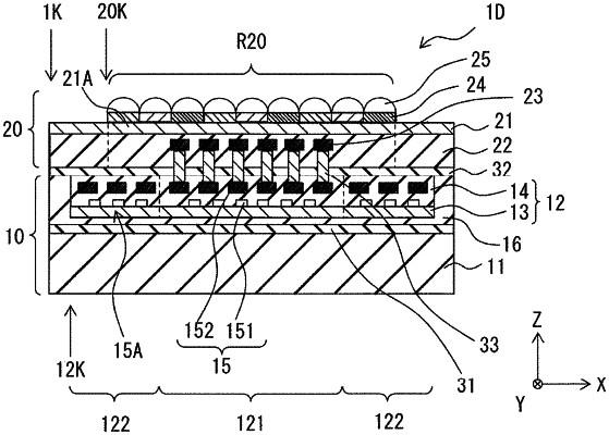
a stacked structure that includes:
a sensor board that includes having an effective pixel region, wherein
the effective pixel region includes an imaging device,
the imaging device includes a plurality of pixels, and
the imaging device is configured to receive external light in each pixel of the plurality of pixels to generate a pixel signal; and
a circuit board that includes a chip, wherein
the chip includes a first portion and a second portion,
the first portion is integrated with the second portion,
the first portion includes a signal processing circuit,
the signal processing circuit includes a first semiconductor device configured to execute signal processing of the pixel signal,
the second portion is at a position different from a position of the first portion in an in-plane direction on the circuit board,
the second portion includes a dummy circuit including a second semiconductor device, and
both the first portion and the second portion overlap the effective pixel region in a stacking direction of the sensor board and the circuit board.
|