| CPC H01L 25/105 (2013.01) [H01L 25/50 (2013.01); H01L 2225/1035 (2013.01); H01L 2225/1041 (2013.01); H01L 2225/1058 (2013.01); H01L 2225/1094 (2013.01)] | 22 Claims |
|
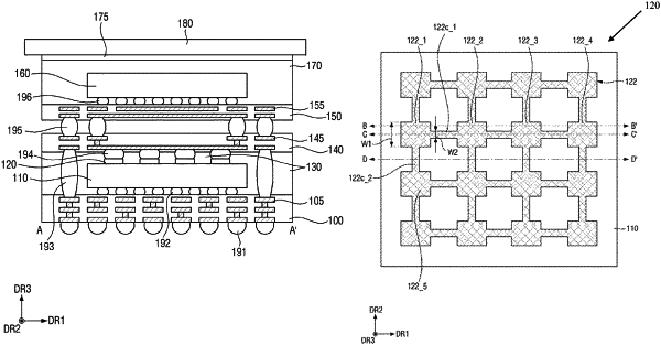
1. A semiconductor package comprising:
a first substrate;
a mold layer provided on the first substrate;
a first semiconductor chip provided on the first substrate;
a heat sink structure comprising a heat sink pattern provided on the first semiconductor chip, a metal film pattern provided on the heat sink pattern, and an insulating film provided on side walls of the heat sink pattern and side walls of the metal film pattern;
an interposer provided on the heat sink structure; and
a solder ball provided to the heat sink structure and the interposer,
wherein the mold layer is provided to surround the insulating film.
|